")

")

 |
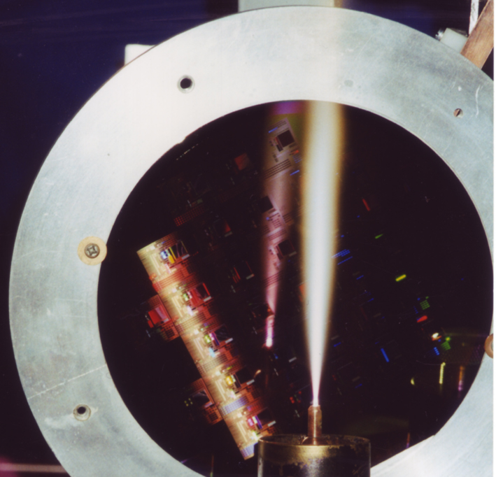
From semi-conductors to printing, including medical applications, food packaging and MEMS – in every domain our Atmospheric Pressure Plasma equipment could be used to solve complex and non-routine issues. Plastics and metals, ceramics and glass, carbon-based materials and semi-conductors, any combination of these materials – there is no restriction for use of our Atmospheric Pressure Plasma technology in any of mentioned situations. Being a key of surface preparation solution, our Atmospheric Pressure Plasma technology brings an essential technical advantage and an additional economic benefit. |
|
| Improving quality of product and effectiveness of manufacturing process without loosing of price competitiveness is mainly done by implementing of new engineering and fabrication procedures. Our leading-edge Atmospheric Pressure Plasma technology gives to our customers powerful tool for reaching their quality and effectiveness objectives. Our equipment is easy to operate , adjust and maintain. It could be used for continuous and batch processing, within high speed manufacturing lines and in piece-by-piece manufacturing processes. Small, easy to integrate into automated production lines, our equipment offers low operating cost and rapid amortization of investment. |
 |
|